Plasma refers to ‘ionized gas.’ When high energy is applied to the gas atoms or molecules, the electrons get knocked off the particles, ionizing the gas. As a result, the particles are divided into positive and negative ions, radicals, and photons – forming plasma
電漿(Plasma)是指「離子化的氣體(Ionized Gas)」。當高能量施加於氣體的原子或分子時,電子會從粒子中分離,使氣體產生離子化。其結果會形成正離子、負離子、自由基(Radical)及光子(Photon)等粒子,進而形成電漿狀態。
The plasma shows apparent neutrality due to the same number of positively and negatively charged particles (Quasi-Neutral). Since plasma possesses free moving electrons and charged particles, it is highly responsive to electric and magnetic fields (Collective Behavior).
由於電漿中的正電與負電粒子在整體上維持平衡,因此表現出近似電中性的特性,此現象稱為 準中性(Quasi-Neutrality)。此外,由於電漿中存在可自由移動的電子與帶電粒子,因此對電場與磁場具有高度反應性,此特性稱為 集體行為(Collective Behavior)。
Nowadays, plasma plays an essential role in many industrial fields. In semi-conductor manufacturing, more than 70% of the process uses plasma. By using the chemical and physical properties of plasma, we can change the surface properties of materials. It is a future-oriented technology with new applications continually being developed.
現今,電漿技術在許多工業領域中扮演著重要角色。尤其在半導體製造過程中,許多關鍵製程皆廣泛應用電漿技術。透過電漿的化學與物理特性,可對材料表面進行處理,改變其表面特性或賦予新的功能。
電漿技術目前廣泛應用於半導體、顯示器、電子元件、材料及表面處理等領域,並持續發展新的應用,是一項具有高度發展潛力的未來關鍵技術。

Types of Plasma Systems
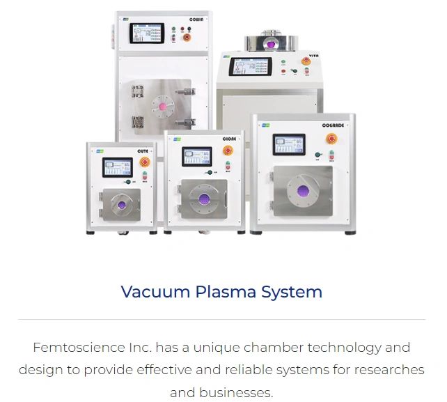
Co-Series
CUTE / CONVANCE / COGRADE
Vacuum Plasma System – Table top
(Plasma Surface Treatment)

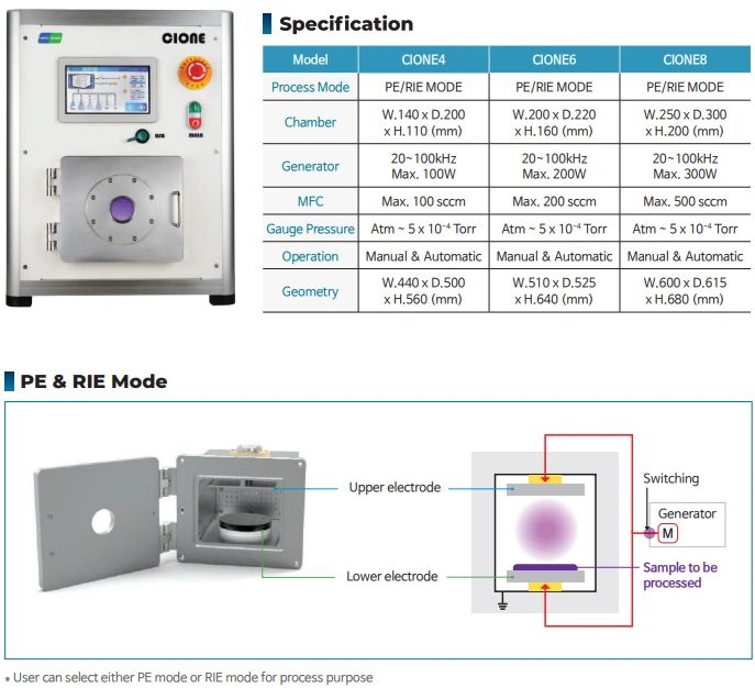
CIONE Series
Dual-Mode Vacuum Plasma System
(Plasma Etching & Reactive Ion Etching)
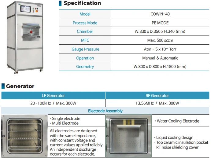
COWIN
Vacuum Plasma System
For Batch Processing
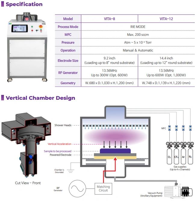
VITA
Vertical Chamber Vacuum Plasma
(Reactive Ion Etching)
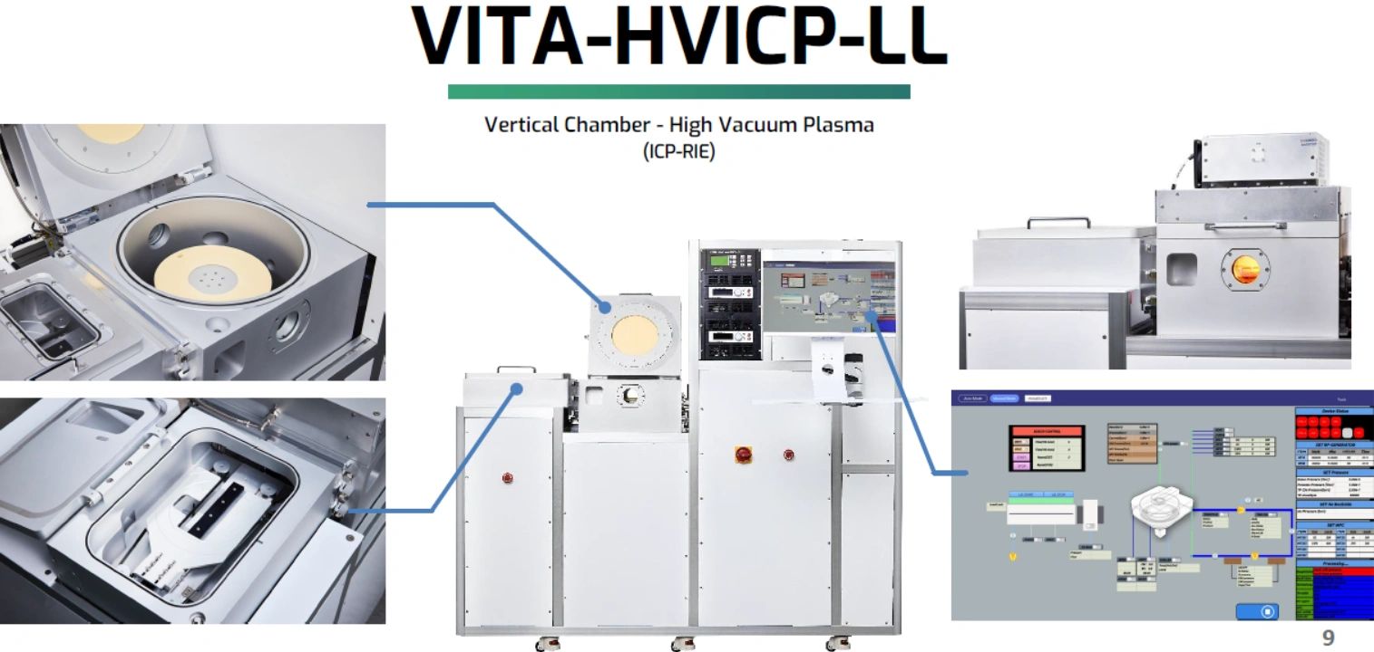
VITA-HVICP-LL
Vertical Chamber - High Vacuum Plasma
(ICP-RIE)
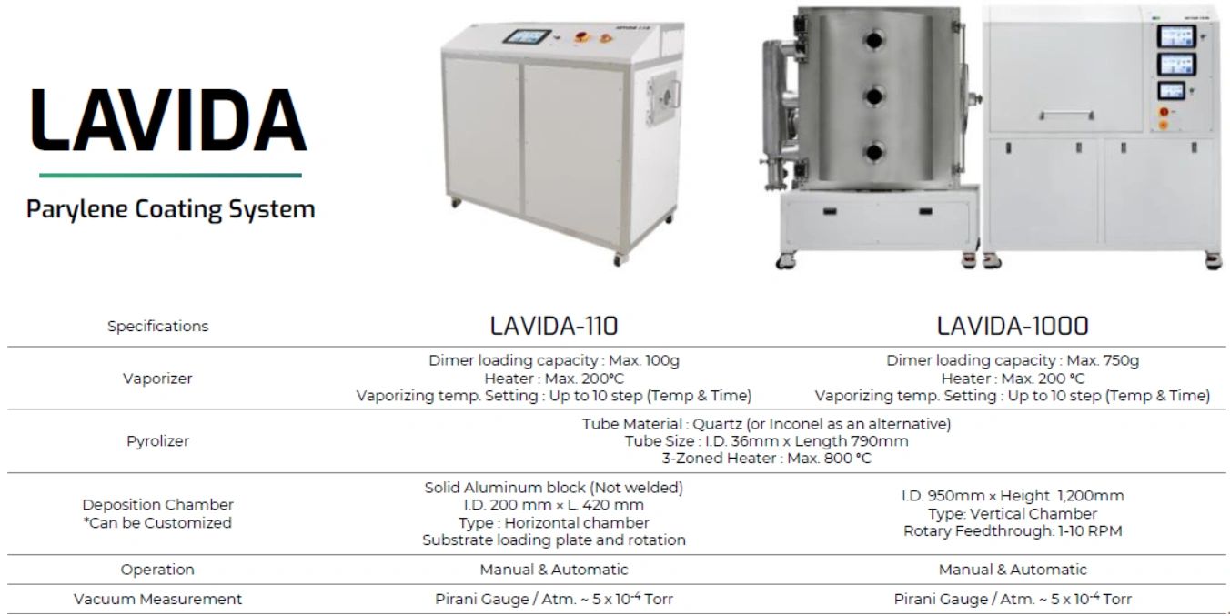
LAVIDA
Parylene Coating System
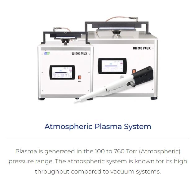
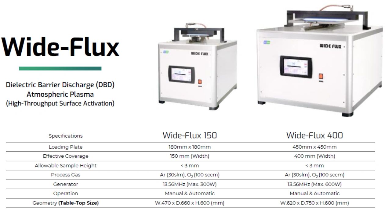
Wide-Flux
Dielectric Barrier Discharge (DBD)
Atmospheric Plasma
(High-Throughput Surface Activation)
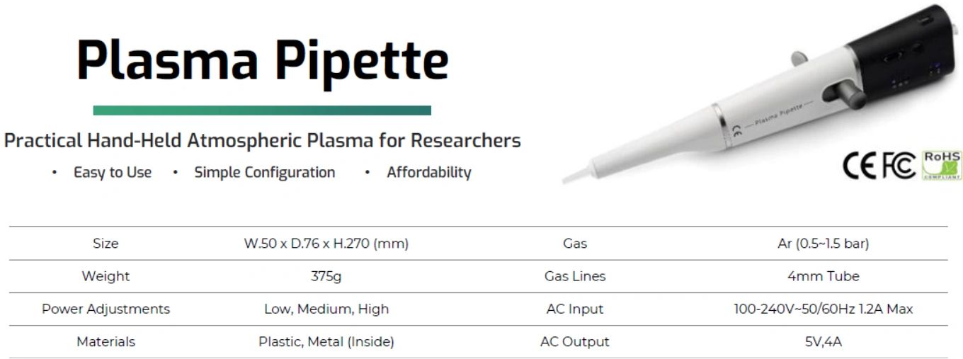
Plasma Pipette
Practical Hand-Held Atmospheric Plasma for Researchers
• Easy to Use
• Simple Configuration
• Affordability